High-energy electrons reveal hidden speed in radiation detectors
Clustering electrical charges could allow sensors to register ionizing radiation almost instantaneously, pointing toward sharper medical scans and faster scientific instruments.
When high-energy radiation crashes into solid matter, the collision dislodges electrons from atoms and leaves behind an invisible trail of energetic disturbance.1 For decades, measuring that disturbance has forced a compromise. Instruments that capture bright signals typically take considerable time to gather and release their light, while devices designed for speed deliver faint pulses that struggle to rise above background noise.1 That persistent friction between timing and brightness has shaped everything from airport luggage scanners to hospital diagnostics.
Radiation detection touches everyday life primarily through healthcare and industrial safety.1 In positron emission tomography, known as a PET scan, doctors inject a patient with a radioactive tracer that emits positrons as it decays.1 These positrons collide with electrons to produce gamma rays that penetrate outward through tissue and strike surrounding detector crystals.1 The quality of the resulting diagnostic scan depends entirely on how quickly and clearly those crystals record each departing ray.
To capture radiation that human senses cannot register, detectors rely on a precise chain of events.1 An incoming particle or gamma ray must first slam into a detection medium, expelling electrons from host atoms in an ionization cascade.1 Those liberated electrons and their corresponding vacant spaces, called electron-hole pairs or charge carriers, then drift through the material before recombining.1 Finally, as the carriers settle, the medium releases a secondary burst of visible light or electric current that sensors record as a detection event.1 When this cascade unfolds slowly, timing precision slips, yet speeding it up traditionally means sacrificing signal strength.
Researchers at Stanford University and the Department of Energy's SLAC National Accelerator Laboratory found that this trade-off is not an absolute barrier.1 In a study published in the journal Nature Photonics, the research team discovered that exposing materials to high-energy electrons generates unexpectedly strong optical signals on ultrafast timescales.1 The charge carriers created during the process do not disperse smoothly across the lattice as long-standing assumptions predicted.1 Instead, they gather into dense, localized pockets that fundamentally change how the host material transmits light.1
How do charge carriers reshape a material?
The sudden crowding of dislodged charges alters the underlying electronic landscape of the material.1 In an ordinary semiconductor, a fixed energetic threshold known as the band gap determines which wavelengths of light can pass through and which wavelengths are absorbed.1 The band gap represents an energy zone where no electronic states can exist, functioning like a forbidden zone for passing photons.1 When the high-energy electron beam ionized the sample, the sheer concentration of charge carriers packed together so tightly that it pushed the band gap to a different energy level.1
This energetic shift allowed the material to transmit optical wavelengths that it would normally absorb.1 Diana Jeong, an instructor of radiology at Stanford University and corresponding author of the study, had prepared for a much more uniform reaction across the crystal.1 Jeong compared the expected distribution of charges to a chocolate brownie, where ingredients blend evenly throughout, but observed instead a pattern resembling a chocolate chip cookie studded with intense clumps of energy.1 "It was very weird," Jeong said.1 "The densities were much higher than we calculated."1
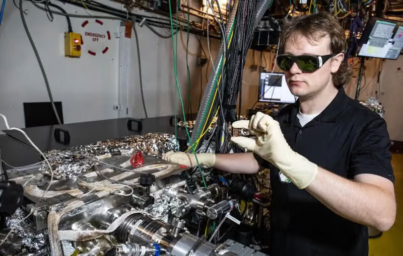
The physical consequence of this clumping is a dramatically magnified optical response that emerges within femtoseconds of the initial collision. Because the localized carrier density spikes so sharply, the optical properties of the material swing far more violently than previous linear models anticipated. Tom Hopper, an assistant professor of chemistry at the University of Central Florida who contributed to the work as a postdoctoral scholar at SLAC, pointed to the resulting optical change as the central surprise.1 "The semiconductor was now able to transmit light where it normally would not be able to because the band gap shifted quite substantially in energy due to some process that has been driven by these high-energy electrons," Hopper said.1
Why invert an electron camera to test the effect?
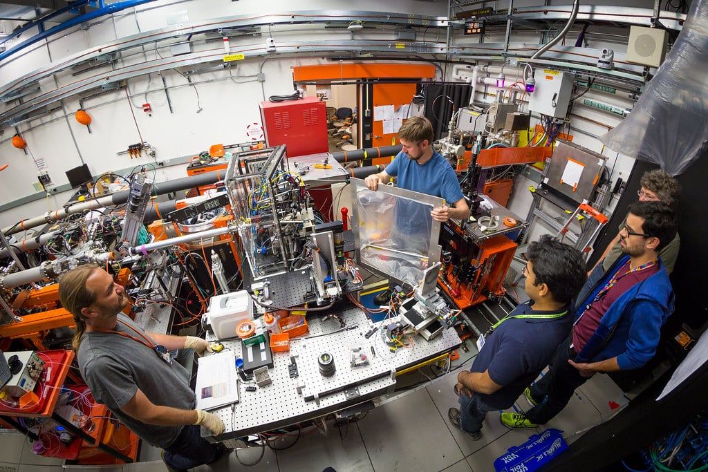
To inspect physical interactions that unfold over fractions of a picosecond, the researchers used the Megaelectronvolt Ultrafast Electron Diffraction instrument, known as MeV-UED, at SLAC's Linac Coherent Light Source facility.1 Scientists usually employ this high-powered instrument as an electron camera, scattering electron bunches off crystalline samples to map the positions of individual vibrating atoms.1 In this investigation, the team reversed that standard operating method by directing relativistic electron bunches straight into the target to act as an ionizing pump source.1
Patrick Kramer, a SLAC staff scientist and the laser science lead for the instrument, explained that the arrangement turned conventional electron diffraction upside down.1 "Normally, we use this system to measure electron diffraction, but this experiment flipped that on its head," Kramer said.1 "It's a microscopy experiment in a different sense."1 The relativistic electron pulses deposited large quantities of energy into target samples of II-VI semiconductors, an established family of electronic materials common in infrared sensors and photovoltaic solar cells.1 While the electron beam supplied the ionizing impact, synchronized optical laser pulses across diverse wavelengths probed the crystal immediately after collision, capturing transient transmission changes before standard fluorescent emission had time to occur.1
The choice of target materials gave the experiment its sensitivity. Common scintillation crystals used in clinical scanners rely on phosphorescence or fluorescence, producing a gradual afterglow that can blur high-speed events.1 In contrast, II-VI semiconductor crystals convert energetic disturbances directly into shifting optical absorption coefficients. "Semiconductors are ideal for a proof-of-concept experiment like this, because they essentially convert this high-energy radiation from electrons into measurable changes in their optical properties," Hopper said.1
What can these laboratory measurements show?
The findings provide an experimental demonstration of charge clustering under focused electron pulses, but they do not describe an off-the-shelf medical instrument.1 The measurements were conducted using a specialized particle accelerator facility that accelerates electrons to megaelectronvolt energies far beyond the operating conditions of standard clinical hardware.1 The study examined specific semiconductor slabs under tightly controlled laser interrogation, which leaves open the question of how alternative detector geometries and lower radiation fluxes will behave.1
Translating these ultrafast optical shifts into compact sensors will require testing whether similar carrier aggregation occurs under broader particle spectra and lower energy thresholds. Jeong noted that the physical mechanism should theoretically persist in lower-energy environments, such as diagnostic imaging equipment that could operate inside a local medical clinic.1 If smaller systems reproduce the same band-gap shifts, instrument designers could bypass the slow glowing phase of conventional scintillators entirely.1 Detecting radiation through immediate optical switching would allow medical scanners to locate decaying isotopes with millimeter accuracy while exposing patients to lower overall doses.1
For now, the work reframes how physicists model high-energy radiation damage and electronic relaxation in crystalline solids. The discovery demonstrates that energy deposition across dense lattices is intrinsically non-uniform on early timescales, offering a path to build radiation sensors that are both extremely sensitive and exceptionally fast.1 "Our hope is that this leads to new sensing platforms that can form images right away and lead to real-time intervention," Jeong said.1
What this rests on
42 sentences trace to 1 source.
-
1
N
Newswise Document · newswise.com Ultrafast Electrons and Lasers Open Possibilities for Better Imaging and Sensing Technologies See the source