Artificial intelligence learns to assemble designer materials atom by atom
Autonomous molecular positioning allows microscopic needles to construct synthetic graphene frameworks without continuous human supervision, opening direct paths toward custom electronic materials.
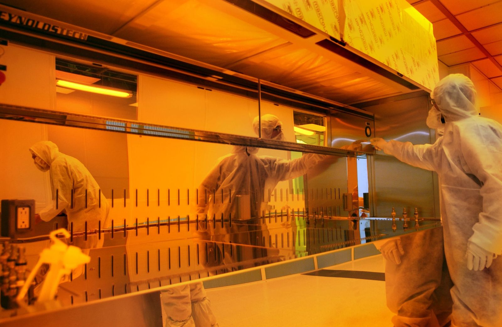
Solid matter owes its electronic behavior to the geometric arrangement of its constituent parts. When atoms or molecules settle into regular, repeating geometric frameworks known as crystal lattices, their shared electrons travel along paths dictated entirely by that spatial pattern. In natural crystals, chemistry and thermodynamics set those boundaries, leaving scientists to discover whatever properties nature happens to provide. Rearranging individual molecules by hand to test theoretical geometries has historically posed an excruciating physical barrier, because nudging components into place across a surface requires guiding an unimaginably sharp tip without breaking it against adjacent atoms.
That manual bottleneck has restricted experimental physicists to working through delicate single-atom manipulations where one misplaced movement can blunt or snap the microscopic probe. Moving even a few dozen molecules into an orderly pattern used to demand exhausting, continuous human attention over days of trial and error. The ability to direct electrons into artificial behaviors that do not appear in naturally occurring minerals depends directly on whether researchers can assemble these synthetic molecular grids reliably and repeatedly.
A research team at Oak Ridge National Laboratory has demonstrated an automated platform that delegates this physical assembly to machine learning models, publishing their findings in the journal ACS Nano.1 By pairing real-time computer vision with reinforcement learning algorithms, the system carried out molecular construction continuously across more than 25 hours without direct human steering.1 The experiment marks a shift toward building custom functional matter directly from atomic building blocks.
How can machines assemble matter molecule by molecule?
An automated assembly system must repeatedly identify where a molecule rests, determine how close to nudge it, and deliver an electrical pulse without crushing the tip against the underlying surface. The process operates through a scanning probe, an instrument that uses a needle sharpened to a single atom at its apex to sense and move nanoscale matter. To relocate a molecule, the instrument brings this microscopic tip close to the target, applies a specific electrical bias and current, and drags the molecule across the substrate. If the current is too weak or the movement too quick, the molecule slips away; if the tip presses too hard, the atomic apex deforms and ruins the instrument.
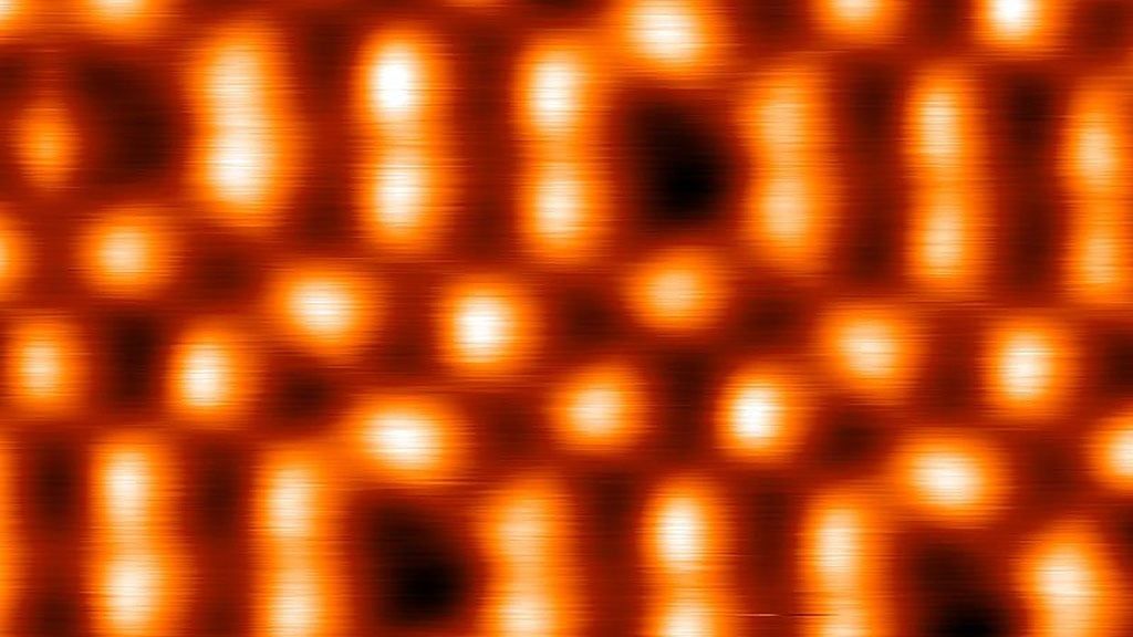
To solve this control problem, researchers at the Center for Nanophase Materials Sciences at Oak Ridge National Laboratory split the physical task into visual perception and tactical decision-making.1 The software relied on an object-detection framework called YOLO, short for You Only Look Once, to scan copper surfaces and locate individual molecules rapidly.1 This visual system functioned as the platform's eyes, identifying the exact coordinates of every loose molecule resting on the metal substrate.
Tactical movement fell to a reinforcement learning algorithm, which served as the operational brain of the apparatus. Reinforcement learning is a computational training method where an algorithm explores different physical choices and receives positive or negative mathematical rewards based on the outcome of each attempt. The system received its highest reward when a targeted molecule reached its intended coordinate and received a substantially reduced score when the nudge missed the mark.1 By analyzing which actions produced higher scores, the software learned the precise combinations of electrical bias, current levels, and lateral manipulation speeds needed to slide molecules smoothly across copper without destroying the microscopic needle.1
What did the automated system construct on the surface?
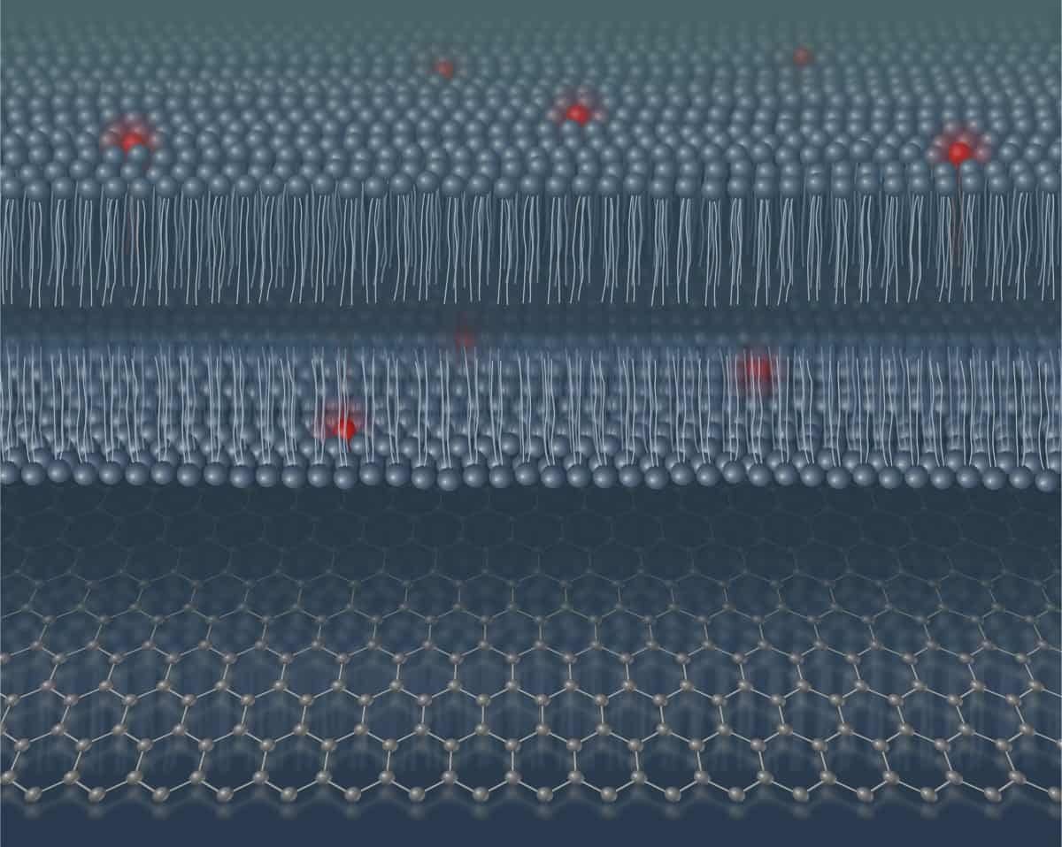
The autonomous assembly platform demonstrated its capabilities by constructing an artificial graphene lattice out of 37 separate molecules arranged on a copper base.1 Natural graphene consists of carbon atoms arranged in a flat, hexagonal honeycomb pattern that grants electrons extraordinary mobility. The researchers configured their system to replicate that geometry synthetically, directing the probe to push molecules into a symmetrical 37-molecule hexagonal grid over hundreds of successive movements.
Physical assembly alone does not guarantee that an artificial lattice will conduct electricity like its natural counterpart, so the researchers verified the structure's physical behavior using spectroscopic measurements. Spectroscopy examines how matter absorbs, reflects, or emits energy to reveal its internal electronic states. The diagnostic scans detected a Dirac point, a distinctive electronic signature where energy bands meet in a cone shape, confirming that electrons moving through the synthetic molecular grid behaved exactly like charge carriers in natural graphene.1 To illustrate that the automated system could follow arbitrary geometric patterns beyond regular lattices, the researchers also instructed the machine to manipulate individual molecules into letters spelling out ORNL across the copper surface.1
The underlying conceptual framework was developed by P. Ganesh and Arthur P. Baddorf, alongside An-Ping Li and Rama Vasudevan, who supervised the experimental implementation and evaluated the physical measurements.1 Software development was led by Ganesh Narasimha, who built the core automation architecture using guidance from Vasudevan.1 Mykola Telychko designed the physical experimental setup and worked alongside Narasimha to conduct the assembly trials and record the operational data.1 Wooin Yang designed the visual detection pipeline and carried out the spectroscopic validation that proved the artificial graphene reproduced real electronic properties.1 Narasimha explained that the unified platform establishes atomically precise fabrication with significantly reduced human input, shifting the field from passive material discovery toward deliberate structural engineering.1
What boundaries still constrain autonomous atomic assembly?
The current platform operates as a semi-automated system because physical wear on the scanning probe still requires human intervention.1 During extended runs, the microscopic apex of the needle can pick up stray atoms or suffer physical instability from surface interactions, forcing an operator to pause the run to condition or repair the tip. The process is also constrained by assembly speed, taking roughly one minute to complete a single molecular nudge. Building the 37-molecule artificial graphene honeycomb required approximately 900 individual algorithmic iterations across 25 hours of operation.1
These experimental results represent a single-instrument laboratory demonstration on a specific copper substrate, rather than an industrial manufacturing process. The system's reinforcement learning policies were tuned to manipulate particular molecules under ultra-high vacuum conditions, meaning the current parameters cannot be assumed to transfer automatically to different atomic species, irregular surfaces, or ambient environments. While the software successfully positioned dozens of molecules, practical microelectronic or computing components will require scaling up assembly throughput by orders of magnitude.
The research was conducted at the Center for Nanophase Materials Sciences, a Department of Energy user facility managed by UT-Battelle at Oak Ridge National Laboratory, with experimental funding from the Basic Energy Sciences Scientific User Facilities Division under the Quantum Information Science Infrastructure Project.1 The scientists plan to use this baseline to pursue inverse design, a workflow where researchers specify an electronic property in advance and allow algorithms to determine and construct the required atomic lattice. Applying this automated precision to artificial lattices provides an experimental testbed for topological qubits, which serve as foundational building blocks for fault-tolerant quantum computers.1
What this rests on
18 sentences trace to 1 source.
-
1
N
Newswise Document · newswise.com AI Automates the Creation of Custom Materials See the source